


![[Day2]Panoramic VR takes you to the “cloud” of the World Manufacturing Conference](https://img.chinait.com/chinait-en/2021/11/193033.jpg)


(ChinaIT.com News) Recently, Microconductor Nano released official news that the company’s first semiconductor CVD thin film deposition equipment was successfully delivered.
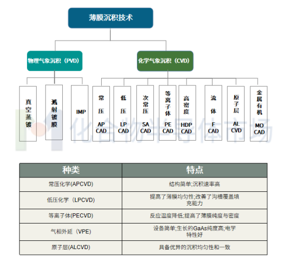
Thin film deposition is divided into two categories: physical vapor deposition (PVD) and chemical vapor deposition (CVD). The former uses physical methods (such as evaporation, sputtering, etc.) to vaporize the coating material and deposits a film on the surface of the substrate. The latter uses gaseous or vaporous substances to react on the gas phase or gas-solid interface to form solid deposits. The current SiC film growth is mainly based on CVD, including molecular beam epitaxy, magnetron sputtering and pulsed laser deposition, etc. The advantages of CVD are that it can accurately control the epitaxial film thickness and doping concentration, fewer defects, moderate growth rate, and automatic process control. It is a SiC epitaxy technology that has been successfully commercialized. To evaluate the core indicators of a silicon carbide CVD, it is mainly judged from three aspects: epitaxial growth performance (thickness uniformity, doping uniformity, defect rate and growth rate), temperature performance of the equipment itself (heating/cooling rate, maximum temperature, temperature uniformity), and equipment cost performance.
 From the perspective of the entire semiconductor industry, the current domestic CVD localization rate is still at a relatively low level. From the perspective of the entire semiconductor market, Applied Materials, Lam Research in the United States and Tokyo Electron (TEL) in Japan are the main suppliers of CVD in the world.
In the field of silicon carbide, only the epitaxial link is considered. The main suppliers of CVD equipment are Aixtron in Germany, LPE in Italy, Tokyo Electron (TEL) and Nuflare in Japan.
And according to relevant information, 6-inch epitaxy equipment is concentrated in LPE in Italy and NuFlare in Japan, and NuFlare is mainly supplied to Wolfspeed and II-VI (renamed Coherent), and the number is only a dozen units per year. Its sales in China have been scheduled until the second half of 2023, and the design capacity of each unit is 1,800 pieces/month. The equipment of Japan’s Tokyo Electronics (TEL) mainly uses dual chambers, which has a certain effect on increasing production, but due to issues such as price and technical IP, it seldom appears in the domestic market.
In February of this year, Jingsheng Electromechanical released a 6-inch double-chip SiC epitaxial equipment. Through the transformation of the graphite parts in the reaction chamber, the equipment adopts the method of superimposing the upper and lower layers. A single furnace can grow two epitaxial wafers, and the process gas of the upper and lower layers can be controlled separately.
In May, Yuesheng Company announced that its self-developed 4/6-inch SiC epitaxial equipment has been running continuously and stably for nearly 300 hours without failure, and the quality of the grown 4/6-inch SiC epitaxial wafers has reached the international advanced level, meeting the preparation requirements of MOSFET and SBD devices.
In the same month, the “Great Wall Holdings Bidding Center” issued a document stating that it had launched the “Seiko Automation Silicon Carbide Epitaxy Plant Renovation Design Project” and is currently bidding.
In addition, the Yandu District People’s Government of Yancheng City reported that Hanyin Electromechanical invested 1 billion yuan in 2022 to start the Hanyin semiconductor equipment project, and newly installed 40 sets (sets) of third-generation semiconductor carbon epitaxy equipment, which can produce 200,000 silicon carbide epitaxial wafers per year.


